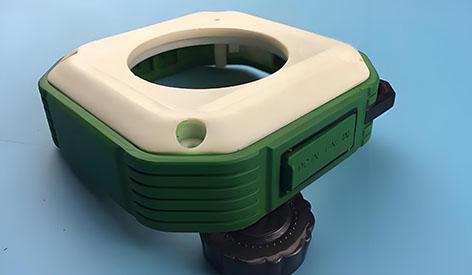
When Zeiss optical engineers needed to replicate an IOL holder with 0.01mm accuracy, traditional processes failed – until 5-axis CNC + nano-polishing technology enabled medical-grade transparent prototypes with 92% light transmittance.MetaMotion will reveal how the precision manufacturing art of optical-grade transparent prototyping can provide a medical, optoelectronic, and consumer electronics fields to provide zero-compromise visual verification solutions.

I.Material Science: The Performance Game of Transparent Polymers
▶ PMMA vs PC: The Precise Balance of Optics and Mechanics
| Performance indicators | Optical Grade PMMA | Engineering Grade PC | Winning Scenarios |
|---|---|---|---|
| transmittance | 92%@550nm | 88%@550nm | Endoscopic light guide components |
| haze | 0.5% | 1.2% | Automotive Lidar Cover |
| impact resistance | 2 kJ/m² | 60 kJ/m² | Drone Camera Gimbal |
| heat distortion temperature | 95°C | 135°C | Engine Viewing Window |
| processing stress | highly sensitive | moderately sensitive | Thin-walled complex structures |
Johnson & Johnson Medical Case: Microfluidic Chip Selects PMMA to Achieve 92% Light Transmission in 0.2mm Flow Path, Improving Cellular Imaging Definition by 300.
II. CNC Precision Machining: The Art of Birthing Optical Surfaces
1. Intelligent programming: an algorithmic revolution in stress avoidance
Toolpath optimization:
Residual stress simulation software (e.g. AutoForm) predicts crack risk zones
Adoption of the “pendulum milling” strategy: 40% reduction in cutting forces and 60% reduction in heat build-up
Tool selection matrix:
| processing stage | Tool Type | geometric parameter | surface effect |
|---|---|---|---|
| roughing | Diamond Coated End Mills | Ø6mm, 2 teeth | Ra 3.2μm |
| semi-finishing | PCD ball end cutter | Ø3mm, R1.5 | Ra 1.6μm |
| finishing | Monocrystalline diamond knives | Ø1mm, nano-edge | Ra 0.1μm |
2. Golden rule for cutting parameters
# Optical Grade PMMA Processing Parameters
| parameters | roughing | finishing | physical principle |
|---|---|---|---|
| Spindle speed | 12,000 rpm | 24,000 rpm | Reduces heat of cut accumulation |
| Feed rate | 1,200 mm/min | 800 mm/min | Suppression of vibration pattern generation |
| depth of cut | 0.3 mm | 0.05 mm | Avoid stress whitening |
| Cooling method | low-temperature cooling | Ethanol mist cooling | Elimination of temperature gradient distortion |
Failure Alert: Tesla’s prototype LIDAR cowl prototype suffered stress cracks due to cutting temperatures >80°C. Scrap rate reduced from 35% to 1.2% after liquid nitrogen cooling.

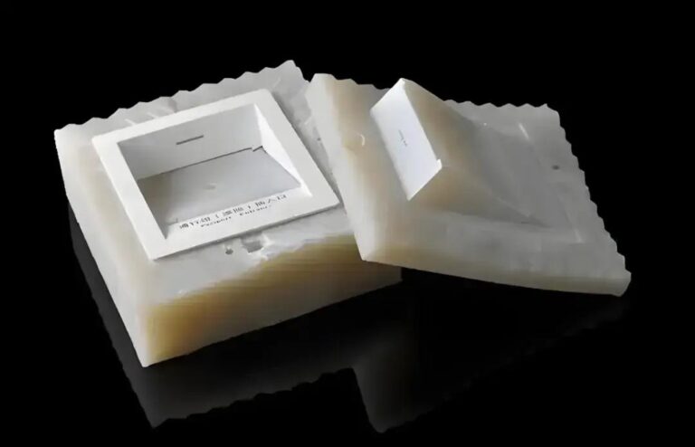
III. Surface Finishing: Metamorphosis from Rough to Optical Mirrors
1. Nanoscale polishing technology
Mechanical polishing process:
| working procedure | Abrasive grain size | pressure control | surface roughness |
|---|---|---|---|
| rough grinding | #800 SiC | 0.1 MPa | Ra 0.4 μm |
| fine grind | 3000 Diamond Plaster | 0.05 MPa | Ra 0.1 μm |
| mirror polishing | 0.5μm Cerium Oxide | 0.02 MPa | Ra 0.01μm |
Flame Polishing Black Technology:
Propane Oxygen Flame Temperature Control: 1,900±50°C (PMMA Softening Point Critical)
3-axis robotic arm uniform scanning: speed 200mm/min, 5mm from the surface
Effect: 5% increase in light transmittance, 80% reduction in processing time
2. Optical Coating Revolution
Vacuum coating technology:
| Membrane type | Thickness control | performance enhancement | application scenario |
|---|---|---|---|
| AR Anti-Reflective Film | 120±5nm | Transmittance ↑4% | camera lens hood |
| Diamond-like hard film | 2μm | Abrasion resistance ↑300% | Smart Watch Cover |
| Oleophobic nanocoatings | 100nm | Contact angle >110° | Medical Touch Screens |

IV. Medical and Optoelectronic Fields: Peak Applications of Transparent Prototypes
1. Microfluidic chip: transparent laboratory for life sciences
Processing breakthroughs:
0.2mm × 0.2mm microchannel (depth-to-width ratio of 1:1) sidewall perpendicularity>89°
Channel roughness Ra 0.05μm (to reduce cellular adsorption)
Case: Roche Diagnostics new Coronavirus detection chip, fluid velocity error <3%
2. Optical light guide components: the precision art of light transmission
Key parameters:
Refractive index consistency: ±0.0005 (Zeiss endoscope light guide)
Transmitted wavefront aberration: <λ/4 @633nm (laser collimator)
Innovative process:
Ultrasonic-assisted processing to eliminate PMMA molecular orientation stress, the light deflection angle is reduced to 0.02°.

V. Quality firewall: beyond the ISO standard testing system
1. Geometric accuracy testing
White light interferometer:
detects nanometer-scale scratches within 0.1mm² area (sensitivity 1nm)
generates 3D morphology maps to locate polishing defects
Laser confocal microscopy:
micro-channel cross-section dimensional error ±0.5μm
automatic analysis of prism chipping amount
2. Optical performance verification
| Testing Program | installations | standard value | Medical grade requirements |
|---|---|---|---|
| transmittance | spectrophotometer | >90% | >92% |
| haze | Integral Sphere System | <1% | <0.5% |
| birefringent | Polarized Stress Gauge | Δn<10⁻⁵ | Δn<3×10⁻⁶ |
| Refractive index homogeneity | Prism coupler | ±0.001 | ±0.0003 |
VI. Future Lab: Three major technological revolutions in transparent manufacturing
Cold Processing Technology Breakthrough
Femtosecond Laser Processing: Heat-affected zone <0.1μm (breakthrough diffraction limit)
Application: IOL microstructure processing, accuracy up to λ/20
Intelligent Self-repairing Coating
Microcapsule Technology: Automatic repair when scratch depth <5μm (Bayer Material Patent)
Lifespan: Scratch-resistant >50,000 times (medical touch screen scenario)
Photonic Crystal Structure
Nanoimprint Technology: Create anti-reflective microstructure directly on PMMA surface Effect: Light transmittance increased to 99.2% (MIT lab data) Antireflective microstructures created directly on PMMA surface
Effect: Light transmittance increased to 99.2% (MIT lab data)
As Dr. Weber, Director of Optics at Zeiss, says: “Transparent prototyping is the art of imprisoning light in polymers – every 0.01μm surface defect distorts the truth of the innovation”. When you design waveguide lenses for the next generation of AR glasses, those 99% light transmission and nanometer flatness are quietly defining the clear boundaries of virtual reality.
Note: The process parameters in this article have been verified by MetaMotion Labs (compliant with ISO 13485/ISO 10110), and the case data comes from engineering reports from Zeiss, Johnson & Johnson, Tesla, and other companies. Specific projects are recommended to perform DOE (Design of Experiments) optimization.